GeezerVisonThe World Wide Web, restored to 800 pixels of glory. | ||||||||||||||||||||||||||||||||||||||||||||||||||||||||||||||||||||||||||||||||||||||||||||||||||||||||||||||||||||||||||||||||||||||||||||||||||||||||||||||||||||||||||||||||||||||||||||||||||||||||||||||||||||||||||||||||||||||||||||||||||||||||||||||||||||||||||||
| Home|About|Gaming cabinet|Archives|How it works|Starter sites | ||||||||||||||||||||||||||||||||||||||||||||||||||||||||||||||||||||||||||||||||||||||||||||||||||||||||||||||||||||||||||||||||||||||||||||||||||||||||||||||||||||||||||||||||||||||||||||||||||||||||||||||||||||||||||||||||||||||||||||||||||||||||||||||||||||||||||||
GeezerVison is showing numato.com — 4 Channel Programmable Relay Module | Numato Lab Help Center USB Relay ModulesPopular Search:USB GPIO, USB Relay, FPGA 4 Channel Programmable Relay Module562 views February 18, 2016 admin 0 
1.Introduction
Numato Lab’s 4 Channel Programmable Relay Module is a feature-rich product that can be programmed with Arduino IDE. The USB to Serial Chip FT232RL helps to upload sketches quickly to the board. This programmability gives this board ultimate flexibility compared to other relay modules where features depend on the preprogrammed firmware and offer limited customizability. The onboard programmable relays, digital I/O’s, analog inputs, Real-Time Clock(RTC) and Micro SD memory card slot make this module useful for learning as well as making sophisticated applications. Applications
Board Features
This product is compatible with the following operating systems.
This module has four on board SPDT 12V mechanical relays and associated drivers capable of controlling a large number of devices including lamps, motors, locks etc…(Please see recommendations for using this product with inductive loads elsewhere in this document). By default, the board burned with Arduino Duemilanove w/ Atmega328 boot loader using the Arduino IDE. This module also includes Digital I/Os(multiplexed with PWM outputs), analog inputs, I2C Interface, Real-Time Clock using DS1307, Micro SD Card Slot for storage, these can be accessed over a USB interface and program easily with Arduino IDE for extended functionality. The module communicates with the host PC over a full-speed USB link. When connected to PC, the module will appear as a serial port in Windows Device Manager (or a serial tty device in Linux and Mac). 2.How to Use 4 Channel Programmable Relay Module2.1.Components/Tools RequiredAlong with the module, you may need the items in the list below for easy and fast installation. 1. USB A to Mini B cable. 2.2.Connection DetailsIMPORTANT! Please exercise the utmost caution while working with electrical mains or other high voltages. Failure to comply with safety regulations may result in injury and or death.
 Connection Diagram The above image shows a basic connection diagram that can be used in most of the situations. The connection diagram is the same for both AC and DC loads. Please make sure to use a freewheeling diode or snubber circuit if the load is inductive. More details about using inductive loads are available elsewhere in this document. Use a USB A to Mini B cable for connecting with PC. It is important to make sure that the wires used to connect loads are sufficiently rated to handle the expected load current. Exercise caution while working with high voltages. Short circuits can cause damage to the module and the PC. The following sections identify individual connections in detail. 2.3.USB InterfaceThe onboard full-speed USB controller that helps a PC/Linux/Mac computer to communicate and control this module seamlessly. Use a USB A to Mini B cable to connecting with a PC. By default, the logic section of the module is powered from USB so make sure not to overcrowd unpowered USB hubs. Visit http://numato.com/cables-accessories to buy cables and accessories for this product 2.4.Relay Contacts
2.5.DC Power SupplyThis module uses an external +12V power supply to function properly. External +12V supply can be given through the DC jack on the board. The logic circuit can be powered from USB or onboard 5V regulator from external +12V. The logic circuit uses +5V supply and the relay coils use +12V supply. By default, the board is configured to use the +5V supply from USB. So an external +5V power is not required unless the USB port is unable to supply enough current. In most cases, USB ports are capable of providing enough current for the module. The +12V supply for the relay coils is not optional and the relay will not switch without this supply. Any off the shelf 12V DC power supply can be used for this purpose. Make sure to connect the power supply in correct polarity. If for any reason, an external 5V power supply needs to be used for the logic section of the module, the Jumper V-Select should be configured properly before connecting the power supply. Please refer to the marking on the board for more details. Connecting power supply incorrectly can cause damage to the module and/or other devices
2.6.On Board RelaysThe board has four 12VDC SPDT mechanical relays that can switch up to 10A. The popular ULN2003 IC is used to drive the relays individually, the inputs of the ULN2003 IC are connected to the Atmega328P digital pins(PD2, PD3, PB1, PD7) and the outputs of the ULN2003 IC are connected to relays(0, 1,2 & 3) respectively. Setting HIGH to these digital pins makes corresponding relay ON and Setting these digital pins LOW makes corresponding relay OFF. Sample sketch for testing Relay is available for download on the product page. The table below summarizes the digital I/O’s used for relay triggering.
2.7.Digital I/O'sIn addition to onboard relays, this board has three Digital IO pins that can be used for various custom applications. Digital IO 5th and 6th are multiplexed with PWM outputs. All IO pins support 5V TTL signals. In output mode, each DIGITAL IO can source up to 20mA. So no additional circuitry is needed to drive regular LEDs. A 1.5 K Ohms series resistor is recommended for current limiting when connecting LED to a DIGITAL IO. Sample sketch for testing Digital I/O’s is available for download on the product page. The table below summarizes the Digital and PWM input positions on the header.
2.8.Analog InputThe board has 4 analog input pins multiplexed with ADC. Analog inputs can read voltages at any level between 0 to 5 volts. It is recommended to use a series resistor to protect the input from stray voltages and spikes. The internal Analog To Digital converter supports 10 bits resolution which is adequate for most applications. Sample sketch for testing Analog In is available for download on the product page. The table below summarizes the Analog and ADC input positions on the header.
2.9.Real Time Clock InputThe DS1307 serial real-time clock (RTC) with low power, full binary-coded decimal (BCD) clock/calendar plus 56 bytes of NV SRAM. Address and data are transferred serially through an I2C, bidirectional bus. The clock/calendar provides seconds, minutes, hours, day, date, month, and year information. The end of the month date is automatically adjusted for months with fewer than 31 days, including corrections for leap year. The clock operates in either the 24-hour or 12-hour format with AM/PM indicator. The chip has a built-in power sense circuit that detects power failures and automatically switches to the backup supply. The timekeeping operation continues while the part operates from the backup supply. A sample sketch for exercising RTC is available for download on the product page. The table below summarizes the I2C pins used for RTC functioning.
2.10.Micro SD Card SlotThe Micro SD uses SPI Communication which uses digital pins PB3(11), PB4(12), and PB5(13) of Atmega328P with MOSI, MISO, & SCK. The CS pin is connected to the PB0(8) of the Atmega328 digital pin. Please refer to the following link for important notes on working with Micro SD Card on this board http://arduino.cc/en/Reference/SDCardNotes. Sample sketch for test Micro SD Card is available for download on the product page. The table below summarizes the SPI pins used for Micro SD Card functioning.
2.11.I2C InterfaceUsing this interface the board can communicate with a wide variety of chips that support I2C communication. Interfacing with various shields, sensors, etc is major applications of this. The table below summarizes the I2C input positions on the header. RTC and these pins both share the same I2C channel.
2.12.In System Programmer (ISP)ISP on the board can act as an AVR ISP. This feature helps to program boot loader on to AVR(Atmega168/Atmega328). For additional information on burning the boot loader, see this link http://arduino.cc/en/Tutorial/ArduinoISP. The ISP pins PB3, PB4, PB5 can also be used as digital I/O’s.
3.Driver Installation3.1.Installing on Windows
The following video demonstrates how to install the driver on Windows 10. 3.2.Installing on LinuxPlease visit the page http://www.ftdichip.com/FTDrivers.htm for more information about drivers for 3.3.Installing on MacSimilar to Linux, Mac operating system comes with the required drivers pre-installed. When connected 4.Powering up Programmable Relay Module 4 Channel1. Select the appropriate jumper selection on the V-Select (Default jumper settings should work in most situations).
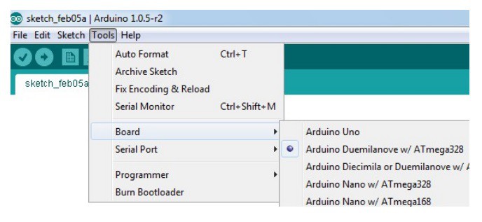
8. Also, select the serial port from the Tools menu (see the image below)
9. Compile and upload code to the board. These commands will work only if the relay control sketch is uploaded to the board.
5.Additional Information5.1.Analog to Digital Converter4 Channel Programmable Relay Module does support Analog to Digital Conversion on some of the IO terminals. A list of analog input pins that supports analog function in this product is listed in Analog Input in this document. There is no special command is required to execute to switch between analog and digital mode. The input voltage range of the ADC is 0 – VDD (this product uses a 5V power supply, so the range will be 0 – 5V). The result will be returned as a number starting at zero and ending at 1023. Zero indicates zero volts at the ADC input and 1023 indicates VDD (5V for this product) at ADC input. 5.2.Using DIGITAL I/Os with SwitchesIt is possible to read the position of a switch that is connected to a DIGITAL IO. An SPST or SPDT switch is recommended to use with DIGITAL IOs. Push switches do maintain the contacts closed only for a very short time so using them is discouraged. The fundamental idea of using a switch with DIGITAL IO is to have the switch cause a voltage level change at the DIGITAL IO pin when pressed. Usually, this is achieved by using an external pull-up resistor along with the switch. The pull-up resistor is connected between the DIGITAL IO and VDD and the switch is connected between the DIGITAL IO and ground. When the switch is not pressed, the pull-up resistor will cause the DIGITAL IO to stay at the VDD voltage level. When the switch is pressed, the DIGITAL IO is short-circuited to ground and stays at zero voltage. This change in voltage and thus the position of the switch can be read using the “DIGITAL IO read” command. Please see the recommended connection diagram below.
5.3.Using Relay Modules with Inductive LoadsIt is important to take additional care when using relays with inductive loads. An inductive load is pretty much anything that has a coil and works based on magnetic principles like Motors, Solenoids, and transformers. Inductive loads produce back emf when the magnitude of the load current changes. The back emf can be in the order of tens or even hundreds of voltage (See this Wikipedia article http://en.wikipedia.org/wiki/Counter-electromotive_force). This effect is most severe when power is disconnected from the inductive load because the rate of change of current is maximum at that point. Even though the back emf lives only for a very short time (a few milliseconds) it can cause sparks between the relay contacts and can deteriorate the contact quality over time and reduce the life span for the relays considerably. So it is important to take countermeasures to suppress the back emf to acceptable levels to protect relay contacts. Usually, this requires connecting electronic devices in parallel with the load such that they absorb the high voltage components generated by the load. For solenoids, connecting a diode (fast switching diode is recommended) in parallel to the load (in reverse direction to the load current) is very effective. A diode used for this purpose is usually called a freewheeling diode. Please see the diagram on the right for connection details.
A capacitor with a proper rating is recommended for protecting the relay contacts when a motor is used as a load. The capacitor should be rated enough to withstand the back emf that is generated by the motor. Please see the diagram below for connection details.
Please note that the relay modules are NOT shipped with back emf suppression devices pre-installed. The exact kind of suppression device and the parameters of the selected device can vary depending on the load itself. Some of the parameters that affect the suppression device selection are the inductance of the load, power supply voltage, load current, physical size/structure of the load, etc.. It is obvious that it is impossible for us to predict these parameters and design required back emf suppression device and incorporate that on the board. So we believe this is a task best left to the module user. There is an excellent article on designing back emf suppression on Wikipedia at http://en.wikipedia.org/wiki/Flyback_diode 6.Technical Specifications
7.Frequently Asked Questions (FAQs)Q. What are the serial parameters I need to use when communicating with this board? Q. Where do I find driver for this product? Q. The DIGITAL IO loses its previously set value when trying to read the status. Why it is so? Q. What is the connector marked as ISP on this module? Q. I need a customized version of this product, can Numato do the customization for me? Q. Where can I buy this product? Suggest Edit
| ||||||||||||||||||||||||||||||||||||||||||||||||||||||||||||||||||||||||||||||||||||||||||||||||||||||||||||||||||||||||||||||||||||||||||||||||||||||||||||||||||||||||||||||||||||||||||||||||||||||||||||||||||||||||||||||||||||||||||||||||||||||||||||||||||||||||||||
| You are visitor 01402503 — GeezerVison does not store the pages you look up. Best viewed with Netscape Navigator 4.7 or Internet Explorer 6 at 800×600. No cookies required. | ||||||||||||||||||||||||||||||||||||||||||||||||||||||||||||||||||||||||||||||||||||||||||||||||||||||||||||||||||||||||||||||||||||||||||||||||||||||||||||||||||||||||||||||||||||||||||||||||||||||||||||||||||||||||||||||||||||||||||||||||||||||||||||||||||||||||||||

 All contacts on each relay are available externally on screw terminals for easy user access. The relays are rated for AC and DC supply voltages. Please see the electrical parameter table for more details. Each relay has three contacts(C, NO, and NC). C is the common terminal and is used in both normally open and normally closed positions. The contacts NC and C will be connected when the relay is turned off and will be disconnected when the relay is turned on. And vice versa, the contacts C and NO will be disconnected when the relay is turned off and will be connected when the relay is turned on. The table below summarizes possible relay contact positions.
 This product requires a driver to be installed for proper functioning when used with Windows. The driver package can be downloaded from http://www.ftdichip.com/FTDrivers.htm. To install the driver, unzip the contents of the downloaded driver package to a folder. Attach the USB cable to the PC and when asked by Windows device installation wizard, point to the folder where driver files are present. When the driver installation is complete, the module should appear in Windows Device Manager as a serial port (see the picture on the right). Note down the name of the serial port (COM9). This information is required to control the module from the PC.